Home / ECE / Analog Electronics :: Section 4

ECE :: Analog Electronics

  1. Assertion (A): An op-amp has high voltage gain, high input impedance and low output impedance

    Reason (R): Negative feedback increases output impedance

  2. A.
    Both A and R are correct and R is correct explanation for A
    B.
    Both A and R are correct but R is not correct explanation for A
    C.
    A is correct R is wrong
    D.
    A is wrong R is correct

    View Answer

    Workspace

    Discuss Discuss in Forum


  3. A transistor has a maximum power dissipation of 350 mW at an ambient temperature of 25°C. If derating factor is 2 mW/°C, the maximum power dissipation for 40°C ambient temperature is

  4. A.
    300 mW
    B.
    330 mW
    C.
    350 mW
    D.
    380 mW

    View Answer

    Workspace

    Discuss Discuss in Forum


  5. The output voltage waveform of a CE amplifier is fed to a dc coupled CRO. The trace on the screen will be

  6. A.
    dc output voltage
    B.
    ac output voltage
    C.
    sum of dc and ac output voltage
    D.
    either (a) or (b)

    View Answer

    Workspace

    Discuss Discuss in Forum


  7. In an RC phase shift oscillator, the total phase shift of the three RC lead networks is

  8. A.
    360°
    B.
    180°
    C.
    90°
    D.

    View Answer

    Workspace

    Discuss Discuss in Forum


  9. In the circuit of figure β = 100 and quiescent value of base current is 20 μA. The quiescent value of collector
    current is

  10. A.
    0.2 μA
    B.
    2 μA
    C.
    2 mA
    D.
    20 mA

    View Answer

    Workspace

    Discuss Discuss in Forum


  11. Values of VT at 20°C for an ideal P-N diode

  12. A.
    25.27 mV
    B.
    30.3 mV
    C.
    23 mV
    D.
    50 mV

    View Answer

    Workspace

    Discuss Discuss in Forum


  13. Assertion (A): In an op-amp the voltage gain and band width can be adjusted as per requirement

    Reason (R): Large value capacitor can also be fabricated on a chip

  14. A.
    Both A and R are correct and R is correct explanation for A
    B.
    Both A and R are correct but R is not correct explanation for A
    C.
    A is correct R is wrong
    D.
    A is wrong R is correct

    View Answer

    Workspace

    Discuss Discuss in Forum


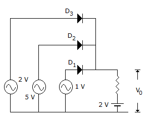
  15. In figure which diode will conduct and what will be the value of V0?
  16. A.
    D3, 1 V
    B.
    D1, 2 V
    C.
    D2, 5 V
    D.
    D1, 5 V

    View Answer

    Workspace

    Discuss Discuss in Forum


  17. For the amplifier circuit of figure, the h parameters of transistor are hib = 25 Ω, hfb = 0.999, hob = 10-6 Ω. The voltage gain is

  18. A.
    0.999
    B.
    1.98
    C.
    20
    D.
    400

    View Answer

    Workspace

    Discuss Discuss in Forum


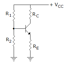
  19. In figure, VCC = + 30 V, R1 = 200 kΩ and R2 = 100 kΩ. If VBE = 0.7 V, the voltage a cross RE =
  20. A.
    +20 V
    B.
    +19.3 V
    C.
    +10 V
    D.
    +9.3 V

    View Answer

    Workspace

    Discuss Discuss in Forum