Home / ECE / Analog Electronics :: Section 14

ECE :: Analog Electronics

  1. Negative feedback is used in audio amplifiers to

  2. A.
    operate class C
    B.
    reduce distortion
    C.
    increase distortion
    D.
    increase gain

    View Answer

    Workspace

    Discuss Discuss in Forum


  3. A BJT amplifier has a power gain of 0.5 from source to base. The power gain in dB is

  4. A.
    -0.3 dB
    B.
    -3 dB
    C.
    -6 dB
    D.
    -10 dB

    View Answer

    Workspace

    Discuss Discuss in Forum


  5. A rectifier circuit has load resistance R. It uses a capacitance filter having capacitance C. For low ripple in the output

  6. A.
    RC should be 1
    B.
    RC should be low
    C.
    RC should be high
    D.
    RC should be neither low nor high

    View Answer

    Workspace

    Discuss Discuss in Forum


  7. In graphical analysis of BJT amplifier the slope of ac line is more than that of dc load line.

  8. A.
    True
    B.
    False

    View Answer

    Workspace

    Discuss Discuss in Forum


  9. Which circuit is called emitter follower?

  10. A.
    CC
    B.
    CE
    C.
    CB
    D.
    Both (a) and (b)

    View Answer

    Workspace

    Discuss Discuss in Forum


  11. Logarithmic amplifiers are used in

  12. A.
    adders
    B.
    dividers
    C.
    multipliers
    D.
    all of the above

    View Answer

    Workspace

    Discuss Discuss in Forum


  13. Figure represents a

  14. A.
    JFET shunt switching circuit
    B.
    JFET series switching circuit
    C.
    JFET analog switch
    D.
    multiplexing

    View Answer

    Workspace

    Discuss Discuss in Forum


  15. In figure VBE = 0.7 V. If base current required to saturate the transistor is 0.1 mA, Vi =

  16. A.
    5 V
    B.
    5.7 V
    C.
    10 V
    D.
    10.7 V

    View Answer

    Workspace

    Discuss Discuss in Forum


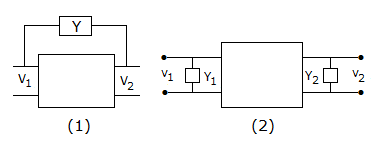
  17. As per miller theorem the circuit of figure (1) can be replaced by that in figure (2) If V1/V2 = K, then Y1 and Y2 are equal to

  18. A.
    Y(1 - K) each
    B.
    each
    C.
    Y1 = Y(1 - K) and Y2 =
    D.
    Y1 = and Y2 = (1 - K)

    View Answer

    Workspace

    Discuss Discuss in Forum


  19. In a biased JFET (Figure) the shape of the channel is as shown because

  20. A.
    it is the property of material used
    B.
    the drain end is more reverse biased than source end
    C.
    drain end is more forward biased than source end
    D.
    impurity profile changes with distance

    View Answer

    Workspace

    Discuss Discuss in Forum