Home / ECE / Digital Electronics :: Section 5

ECE :: Digital Electronics

  1. In a shift left register, shifting a bit by one bit means

  2. A.
    division by 2
    B.
    multiplication by 2
    C.
    subtraction of 2
    D.
    None of the above

    View Answer

    Workspace

    Discuss Discuss in Forum


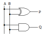
  3. If A = B = 1, the outputs P and Q in the given figure are
  4. A.
    P = Q = 0
    B.
    P = 0, Q = 1
    C.
    P = 1, Q = 0
    D.
    P = Q = 1

    View Answer

    Workspace

    Discuss Discuss in Forum


  5. In the given figure, Y =

  6. A.
    (A + B)C + DE
    B.
    AB + C(D + E)
    C.
    (A + B)C + D + E
    D.
    none of the above

    View Answer

    Workspace

    Discuss Discuss in Forum


  7. Assertion (A): The access time of memory is lowest in the case of DRAM

    Reason (R): DRAM uses refreshing cycle.

  8. A.
    Both A and R are correct and R is correct explanation of A
    B.
    Both A and R are correct but R is not correct explanation of A
    C.
    A is true, R is false
    D.
    A is false, R is true

    View Answer

    Workspace

    Discuss Discuss in Forum


  9. In a 3 input NOR gate, the number of states in which output is 1 equals

  10. A.
    1
    B.
    2
    C.
    3
    D.
    4

    View Answer

    Workspace

    Discuss Discuss in Forum


  11. Assertion (A): Even if TTL gates and CMOS gates used in a realization have the same power supply of + 5 V, suitable circuit is needed to interconnect them

    Reason (R): VOH, VOL, VIH and VIL of a TTL gave are respectively 2.4, 0.4, 2 and 0.8 V respectively. If supply voltage is + 5 V. VIL and VIH for CMOS gate for the supply voltage of + 5 V are 1.5 V and 3.5 V respectively.

  12. A.
    Both A and R are correct and R is correct explanation of A
    B.
    Both A and R are correct but R is not correct explanation of A
    C.
    A is true, R is false
    D.
    A is false, R is true

    View Answer

    Workspace

    Discuss Discuss in Forum


  13. The series 54 H/74 H denotes

  14. A.
    Standard TTL
    B.
    High speed TTL
    C.
    Low Power TTL
    D.
    High Power TTL

    View Answer

    Workspace

    Discuss Discuss in Forum


  15. For a 4096 x 8 EPROM, the number of address lines is

  16. A.
    14
    B.
    12
    C.
    10
    D.
    8

    View Answer

    Workspace

    Discuss Discuss in Forum


  17. Assertion (A): A PROM can be used as a synchronous counter

    Reason (R): Each memory location in a PROM can be read synchronously.

  18. A.
    Both A and R are correct and R is correct explanation of A
    B.
    Both A and R are correct but R is not correct explanation of A
    C.
    A is true, R is false
    D.
    A is false, R is true

    View Answer

    Workspace

    Discuss Discuss in Forum


  19. A B C D + AB C D =

  20. A.
    ABC
    B.
    ABCD
    C.
    A B D
    D.
    ABCD

    View Answer

    Workspace

    Discuss Discuss in Forum