ECE :: Electronic Devices and Circuits
-
The below diagram is __________
- Which of the following are the disadvantages of half wave rectifier
-
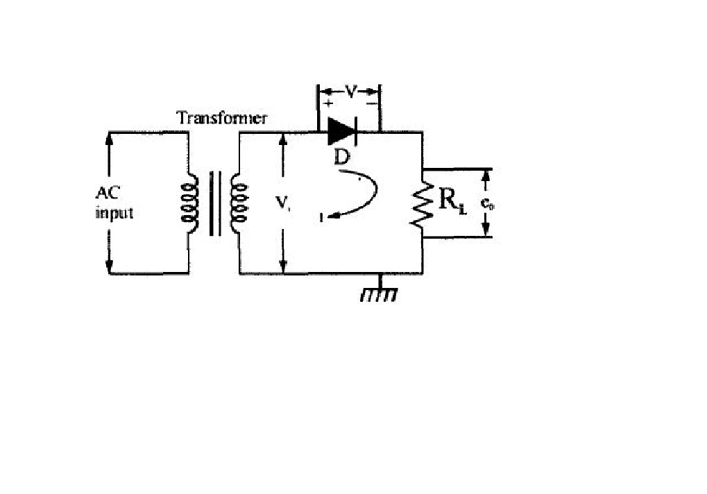
The below diagram is __________

-
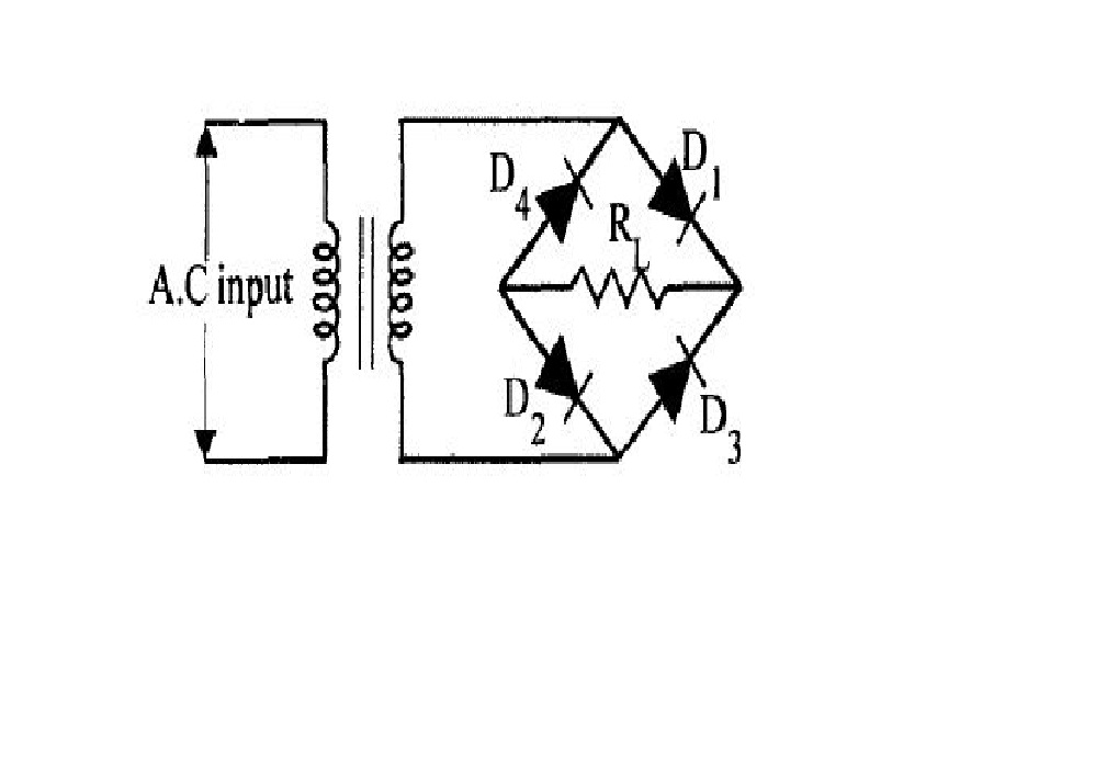
The below diagram is __________
- ________are electronic circuits which give constant DC output voltage, irrespective of variations in Input Voltage V, current drawn by the load I from output terminals
- _____ is a device in which there is a transfer of resistance from input side which is forward biased (low resistance) to output side which is reverse biased (high resistance)
- Which of the following regions are part of the output characteristics of a transistor?
- In which of the following region, both the collector base & base emitter junctions are forward biased ?

 Whatsapp
 Facebook


