Home / ECE / Electronic Devices and Circuits :: Section 9

ECE :: Electronic Devices and Circuits

  1. The O/P char, of a FET is given in the figure. In which region is the device biased for small signal amplification?
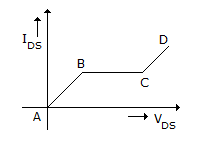
  2. A.
    AB
    B.
    BC
    C.
    CD
    D.
    BD

    View Answer

    Workspace

    Discuss Discuss in Forum


  3. Photoelectric effect occurs only in semiconductors and not in metals.

  4. A.
    True
    B.
    False

    View Answer

    Workspace

    Discuss Discuss in Forum


  5. Which of these has peak and valley points in v-i curve?

  6. A.
    Tunnel diode
    B.
    Zener diode
    C.
    PIN diode
    D.
    Schottky diode

    View Answer

    Workspace

    Discuss Discuss in Forum


  7. The scaling factor of an MOS device using constant voltage scaling model, the gate area of the device will be scaled as

  8. A.
    1/a
    B.
    1/a2
    C.
    1/a3
    D.
    1/a4

    View Answer

    Workspace

    Discuss Discuss in Forum


  9. A full wave bridge rectifier is supplied voltage at 50 Hz. The lowest ripple frequency will be

  10. A.
    400 Hz
    B.
    200 Hz
    C.
    100 Hz
    D.
    50 Hz

    View Answer

    Workspace

    Discuss Discuss in Forum


  11. Electric breakdown strength of a material depends on its

  12. A.
    composition
    B.
    moisture content
    C.
    thickness
    D.
    all of the above

    View Answer

    Workspace

    Discuss Discuss in Forum


  13. The atomic weight of an atom is determined by

  14. A.
    the number of protons
    B.
    the number of neutrons
    C.
    the number of protons and neutrons
    D.
    the number of electrons and protons

    View Answer

    Workspace

    Discuss Discuss in Forum


  15. The minimum charge carried by an ion is

  16. A.
    zero
    B.
    equal to the change of an electron
    C.
    equal to the change of a pair of electrons
    D.
    equal to the change of electrons left in the atom

    View Answer

    Workspace

    Discuss Discuss in Forum


  17. In intrinsic semiconductor at 300 K, the magnitude of free electron concentration in silicon is about

  18. A.
    15 x 104 per cm3
    B.
    5 x 10¹² per cm3
    C.
    1.45 x 10¹⁰ per cm3
    D.
    1.45 x 10⁶ per cm3

    View Answer

    Workspace

    Discuss Discuss in Forum


  19. EG for silicon is 1.12 eV and that for germanium is 0.72 eV. Therefore it can be concluded that

  20. A.
    more number of electron-hole pairs will be generated in silicon than in germanium at room temperature
    B.
    less number of electron hole pairs will be generated in silicon than in germanium at room temperature
    C.
    equal number of electron-hole pairs will be generated in both at lower temperatures
    D.
    equal number of electron-hole pairs will be generated in both at higher temperatures

    View Answer

    Workspace

    Discuss Discuss in Forum