Home / ECE / Electronic Devices and Circuits :: Section 2

ECE :: Electronic Devices and Circuits

  1. The static characteristic of an adequately forward biased P-n junction is a straight line, if the plot is of __________ Vs → versus

  2. A.
    log I Vs log V
    B.
    log I Vs V
    C.
    I Vs log V
    D.
    I Vs V

    View Answer

    Workspace

    Discuss Discuss in Forum


  3. In an n channel JFET

  4. A.
    ID, IS and IG are considered positive when flowing into the transistor
    B.
    ID and IS are considered positive when flowing into transistor and IG is considered positive when flowing out of it
    C.
    ID, IS, IG are considered positive when flowing out of transistor
    D.
    IS and IG are considered positive when flowing into transistor and ID is considered positive when flowing out of it

    View Answer

    Workspace

    Discuss Discuss in Forum


  5. The intrinsic carrier concentration of silicon sample at 300 K is 1.5 x 10¹⁶/m3. If after doping, the number of majority carriers is 5 x 10²⁰/m3. The minority carrier density is

  6. A.
    4.5 x 10¹¹/m3
    B.
    3.33 x 10⁴/m3
    C.
    5 x 10²⁰/m3
    D.
    3 x 10⁻⁵/m3

    View Answer

    Workspace

    Discuss Discuss in Forum


  7. A diode is operating in forward region and the forward voltage and current are v = 3 + 0.3 sin ωt (volts) and i = 5 + 0.2 sin ωt (mA). The average power dissipated is

  8. A.
    15 mW
    B.
    about 15 mW
    C.
    1.5 mW
    D.
    about 1.5 mW

    View Answer

    Workspace

    Discuss Discuss in Forum


  9. Two identical silicon diodes D1 and D2 are connected back to back shown in figure. The reverse saturation current Is of each diode is 10-8 amps and the breakdown voltage VBr is 50 v. Evaluate the voltages VD1 and VD2 dropped across the diodes D1 and D2 assuming KT/q to be 25 m V.
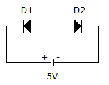
  10. A.
    4.983 V, 0.017 V
    B.
    - 4.98 V, - 0.017 V
    C.
    0.17 V, 4.983 V
    D.
    - 0.017 V, - 4.98 V

    View Answer

    Workspace

    Discuss Discuss in Forum


  11. For BJT transistor. The maximum power dissipation is specified as 350 mW if ambient temperature is 25°C. If ambient temperature is 60°C the maximum power dissipation should be limited to about

  12. A.
    100 mW
    B.
    250 mW
    C.
    450 mW
    D.
    600 mW

    View Answer

    Workspace

    Discuss Discuss in Forum


  13. The concentration of minority carriers in a semiconductor depends mainly on

  14. A.
    the extent of doping
    B.
    temperature
    C.
    the applied bias
    D.
    none of the above

    View Answer

    Workspace

    Discuss Discuss in Forum


  15. Which of the following has highest conductivity?

  16. A.
    Silver
    B.
    Aluminium
    C.
    Tungsten
    D.
    Platinum

    View Answer

    Workspace

    Discuss Discuss in Forum


  17. In a bipolar junction transistor the base region is made very thin so that

  18. A.
    recombination in base region is minimum
    B.
    electric field gradient in base is high
    C.
    base can be easily fabricated
    D.
    base can be easily biased

    View Answer

    Workspace

    Discuss Discuss in Forum


  19. Compared to bipolar junction transistor, a JFET has

  20. A.
    lower input impedance
    B.
    high input impedance and high voltage gain
    C.
    higher voltage gain
    D.
    high input impedance and low voltage gain

    View Answer

    Workspace

    Discuss Discuss in Forum